Detailed Description
Hardware Overview
The figure below illustrates the various hardware components that are located on the top-side of the Ethernet FMC.
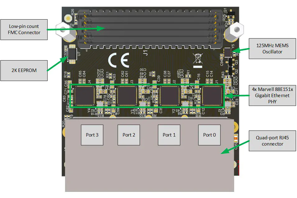
The main components on the top-side of the mezzanine card are:
- 4x Marvell 88E151x Gigabit Ethernet PHYs
- Low Pin Count FMC Connector
- 2K EEPROM
- 125MHz MEMS Clock Oscillator
- 4x 25MHz crystals
- Quad-port RJ45 connector
The figure below illustrates the various hardware components that are located on the bottom-side of the mezzanine card.
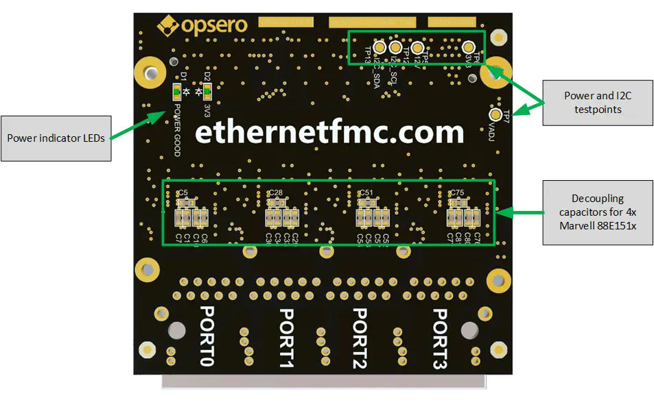
The main components on the bottom-side of the mezzanine card are:
- Decoupling capacitors for the Marvell 88E151x Ethernet PHYs
- Power indicator LEDs
- Test points for power and I2C
Marvell 88E151x Gigabit Ethernet PHY
There are 4x Marvell 88E151x Gigabit Ethernet PHYs on the mezzanine card, one for each of the four Gigabit Ethernet ports. For interfacing with a MAC, the 88E151x has an RGMII (Reduced pin count GMII) interface. The 88E151x is designed for low-power and supports Synchronous Ethernet (SyncE) and Precise Timing Protocol (PTP) Time Stamping. For more specific information on the 88E151x, please refer to the Marvell Marvell 88E151x public datasheet .
In this documentation, we will refer to the PHYs as PHY0, PHY1, PHY2 and PHY3, corresponding to their placement from right-to-left and as shown in Ethernet FMC top labelled image.
Precise Timing Protocol (PTP) Time Stamping Support
The Marvell 88E151x Gigabit Ethernet PHYs support Precise Timing Protocol (PTP). The feature allows time stamping of PTP frames with high precision. The supported time stamping frame formats are as defined in IEEE 802.1AS, IEEE 1588 version 1 and version 2.
The PTP feature can be used on the Ethernet FMC with the following limitations:
An external 125MHz clock cannot be used as the PTP reference clock source. Required PTP control register setting: 20_6.8 = 0 (use internal 125MHz clock). An external PTP reference clock can be supplied to the CONFIG pin of the PHY, but the Ethernet FMC does not make this pin available to the FPGA. The PTP reference clock source must be set to use the internal 125MHz clock.
Capturing of external events via the PTP Event Request input pin is not supported. Required PTP control register setting: 20_6.7 = 0. The PTP Event Request pin (LED1) allows the capture of external events and the recording of the time at which the event occurred, but the Ethernet FMC does not make this pin available to the FPGA, instead it is used to drive the right-side LED of the RJ45.
Generation of an external signal via the PTP Trigger Generate pin is not supported. Required PTP control register setting: 20_6.6 = 0. The PTP Trigger Generate pin (LED1) allows the generation of an external signal when the internal Time of Day counter matches the value in a PHY register, but the Ethernet FMC does not make this pin available to the FPGA, instead it is used to drive the right-side LED of the RJ45.
Generation of an external interrupt via the LED2 pin is not supported. The LED2 pin of the PHY can be used to generate an interrupt signal, but the Ethernet FMC does not make this pin available to the FPGA, instead it is used to drive the left-side LED of the RJ45.
Detailed information on using the PTP Time Stamping feature is contained in the complete datasheet of the 88E151x PHY that is only available through an NDA with Marvell.
RJ45 Connector
The table below lists the RJ45 connectors and Ethernet magnetics used on the Ethernet FMC.
| RJ45 Part number | Magnetics |
|---|---|
| JG0-0025NL | Integrated |
| LPJG48851AFNL | Integrated |
EEPROM
The 2K EEPROM stores IPMI FRU data that can be read by the carrier board and contains the following information:
- Manufacturer name (Opsero Electronic Design Inc.)
- Product name
- Product part number
- Serial number
- Power supply requirements
The FRU data is read by some carrier boards to determine the correct VADJ voltage to apply to the mezzanine card. All Opsero FMC products have their EEPROMs programmed with valid FRU data to allow these carrier boards to correctly power them.
Low Pin Count FMC Connector
The Ethernet FMC has a low pin count FMC (FPGA Mezzanine Card) connector for interfacing with an FPGA or SoC development board. The part number of this connector is Samtec, Low pin count FMC connector, ASP-134604-01 . The pinout of this connector conforms to the VITA 57.1 FPGA Mezzanine Card Standard (for more information, see Pin configuration. For more information on the FMC connector and the VITA 57.1 standard, see the Samtec page on VITA 57.1 .
I/O Interfaces
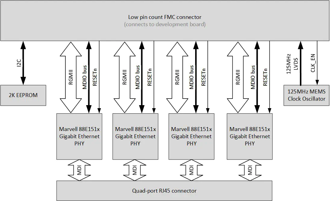
The FMC connector provides power to the Ethernet FMC and also presents the following I/O signals to the FPGA fabric of the development board:
- RGMII for each of the 4x PHYs
- MDIO for each of the 4x PHYs
- I2C for EEPROM R/W access
- Clock enable for 125MHz oscillator
- 125MHz LVDS clock
The figure below illustrates the connections to the FMC connector.
RGMII
The 4x Reduced pin count GMII interfaces form the connection between the Ethernet PHYs and the MACs that are implemented in the FPGA or SoC on the development board. The RGMII interface is a DDR (double data rate) interface that is composed of the following 12 signals:
- Receive data (4 bits)
- Receive clock signal
- Receive control signal
- Transmit data (4 bits)
- Transmit clock signal
- Transmit control signal
MDIO
Each of the 4x MDIO interfaces consist of two signals:
- MDIO Clock signal (driven by the FPGA)
- MDIO Data signal (bidirectional)
The MDIO interface is used to configure the registers of the Ethernet PHYs. More information regarding the 88E151x registers can be found in the Marvell Marvell 88E151x public datasheet .
RESETn
Each of the 4x Ethernet PHYs have an active-low reset input that must be driven by the FPGA.
Power Supplies
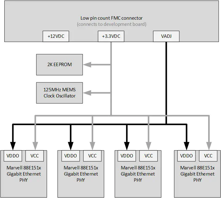
All power required by the Ethernet FMC is supplied by the development board through the FMC connector:
- +12VDC
- +3.3VDC
- VADJ: +2.5VDC or +1.8VDC
3.3VDC Supply
The 3.3VDC supply is the main power supply for the 4x 88E151x Gigabit Ethernet PHYs and it also powers the EEPROM and 125MHz MEMS oscillator.
VADJ Supply
The Ethernet FMC is available in two versions: 1.8V and 2.5V, this corresponds to the VADJ voltage that is required by the board. The difference between the two versions is the part number of the Marvell Gigabit Ethernet PHY that is soldered onto the board. The 1.8V version is loaded with the 88E1518, while the 2.5V version is loaded with the 88E1510.
The VADJ supply is used as the I/O power supply of the 4x 88E151x Gigabit Ethernet PHYs, and this determines the voltage level that must be used by all I/O to and from the PHYs (RGMII, MDIO, RESET_N).
Power LEDs and testpoints
Two LEDs (labelled D1 and D2) on the Ethernet FMC are used to indicate when the required power supplies are active. LED D1 indicates the presence of the 3.3VDC supply and connects to the 3.3VDC power supply through a current limiting resistor. LED D2 indicates the presence of the VADJ power supply and connects to the POWER GOOD signal that is driven by the carrier board and is part of the Vita 57.1 FMC standard.
To aid hardware debug, there is a test point for each of the power supplies on the back side of the Ethernet FMC.
Clocks
The figure below illustrates the clock connections on the Ethernet FMC.
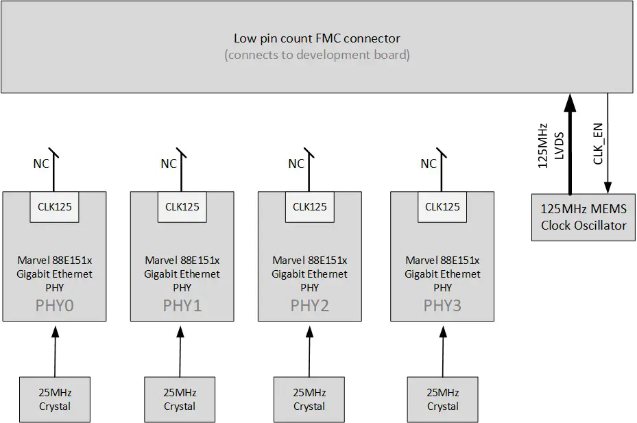
Each of the 4x 88E151x PHYs is connected to a 25MHz crystal for generation of it’s own internal clocks. The Ethernet FMC also has a 125MHz MEMS clock oscillator with LVDS output to provide the FPGA fabric with a precision clock for driving the Ethernet MACs.
Each 88E151x PHY has a CLK125 pin that outputs a 125MHz clock that is synchronized with the 25MHz reference clock. Due to the limited number of pins on the LPC FMC connector, the CLK125 pins are left unconnected on the mezzanine card, hence these clocks are not available to the carrier board.
Resets
The 88E151x Ethernet PHYs each have a hardware reset pin (RESETn) that is routed separately to the FMC connector (see FMC Connector image for details). The reset pin must be driven by the development platform with an active-low signal. There are no pull-up resistors connected to the reset signals on the Ethernet FMC card, and we recommend always driving the reset pins from the development platform in order to ensure reliable reset behavior.
PHY Configuration
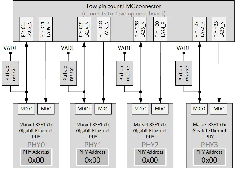
Configuration of the PHY by software is performed using the MDIO bus. The MDIO bus consists of two signals: a bidirectional data signal (MDIO) and a clock signal (MDC). The data signal (MDIO) is driven by the master and slaves as an open drain output, and it is connected to a pull-up resistor located on the mezzanine card. The clock signal (MDC) is driven by the master only (the FPGA on the development platform) and it does not require a pull-up resistor. For more information on the MDIO serial bus standard, please refer to the Wikipedia page on MDIO .
The MDIO bus of each PHY is routed independently to the FMC connector. The PHY address of all PHYs is 0 and the same for all ports (PHY0, PHY1, PHY2 and PHY3).
