Detailed Description
Hardware Overview
The figure below illustrates the various hardware components that are located on the top-side (component side) of the Ethernet FMC Max.
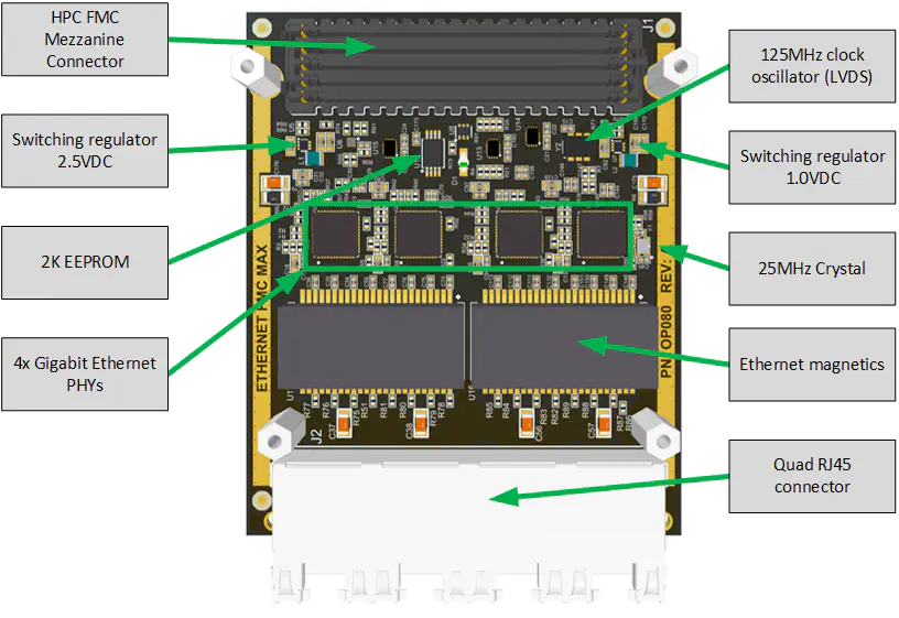
The main components on the top-side of the mezzanine card are:
- 4x TI DP83867 Gigabit Ethernet PHYs
- High Pin Count FMC Connector
- 2K EEPROM
- 125MHz Clock Oscillator
- 25MHz crystal
- Ethernet magnetics
- Quad RJ45 connector
- Switching regulators (1.0V and 2.5V)
- Voltage translators
The figure below illustrates the various hardware components that are located on the bottom-side of the mezzanine card.
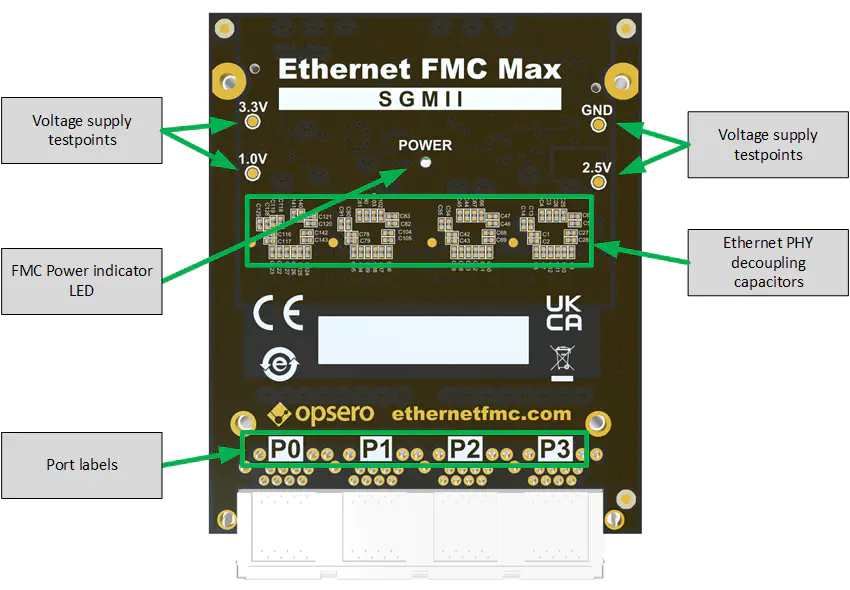
The main components on the bottom-side of the mezzanine card are:
- Decoupling capacitors for the TI DP83867 Gigabit Ethernet PHYs
- Power indicator LED
- Test points for power supplies
- Port labels (P0,P1,P2,P3)
TI DP83867 Gigabit Ethernet PHY
There are 4x TI DP83867 Gigabit Ethernet PHYs on the mezzanine card, one for each of the four Gigabit Ethernet ports. For interfacing with a MAC, the DP83867 has an SGMII (Serial GMII) interface. The DP83867 is designed for low-power, low-latency and features Time Sensitive Network (TSN) compliance, IEEE 1588 Start of Frame Detection and Wake-on-LAN packet detection. For more specific information on the DP83867, please refer to the DP83867 datasheet .
In this documentation, we will refer to the ports and respective PHYs as P0, P1, P2 and P3, corresponding to their placement from left-to-right and as shown in Ethernet FMC Max bottom labelled image.
Strap Configuration
Certain PHY settings are hard wired by resistors connected to “strap” pins of the DP83867 device. These pins determine the value of these settings on power-up of the device, however they can be changed by software by writing to the appropriate PHY registers via the MDIO bus.
The table below describes the strap configuration of the Ethernet FMC Max.
| Strap Pin | Strap Mode | Strap Function |
|---|---|---|
| RX_D0 | 2 (P0) 4 (P1) 1 (P2) 4 (P3) | PHY address [1:0] = 01 PHY address [1:0] = 11 PHY address [1:0] = 00 PHY address [1:0] = 11 |
| RX_D2 | 1 (P0) 1 (P1) 4 (P2) 4 (P3) | PHY address [3:2] = 00 PHY address [3:2] = 00 PHY address [3:2] = 11 PHY address [3:2] = 11 |
| RX_CTRL | 3 | Auto-Negotiation Enable |
| GPIO_0 | 1 | N/A |
| GPIO_1 | 1 | N/A |
| LED_2 | 1 | N/A |
| LED_1 | 1 | Advertise Ability of 10/100/1000 |
| LED_0 | 2 (Rev-A) 4 (Rev-B and up) | Mirror Enable = 0, SGMII Enable = 1 Mirror Enable = 1, SGMII Enable = 1 |
Notes:
- Straps RX_D0 and RX_D2 determine the PHY addresses that are used to target each PHY for MDIO read and writes. More information about configuring the PHYs via MDIO can be found in the MDIO section.
- Straps GPIO_0, GPIO_1 and LED_2 pertain to PHY settings related to the RGMII interface and are not relevant to the Ethernet FMC Max.
- The LED_0 strap on Rev-A boards (serial numbers 800000-800019) is set to mode 2 which disables Mirror Mode. For correct operation of the Ethernet ports on Rev-A boards, the Mirror Mode setting must be enabled by software (write 0x1 to bit 0 of CFG4 register address 0x0031). For more information on enabling Mirror mode, refer to the Mirror mode section of the Programming Guide.
RJ45 Connector and magnetics
The Ethernet FMC Max uses a quad RJ45 connector ( Link-PP, Quad RJ45, LPJE4718AGNL ) and discrete Ethernet magnetics ( Link-PP, Quad Ethernet Magnetics, LP84862ANL ).

As illustrated by the image above, each port on the RJ45 connector has two LEDs, one green and one yellow. The green LED is on the right side of the port (when the tab is pointed up), while the yellow LED is on the left side. The LEDs are connected to the DP83867 PHY as shown in the table below:
| Color | Side | PHY connection | Default operation mode |
|---|---|---|---|
| Green | Right | LED_1 | 1G link established |
| Yellow | Left | LED_0 | Link established |
The operation mode of these LEDs can be changed by writing to the LED Configuration Register (LEDCR1, Address 0x0018) of the TI DP83867 PHY. Refer to the datasheet for more information.
EEPROM
The 2K EEPROM stores IPMI FRU data that can be read by the carrier board and contains the following information:
- Manufacturer name (Opsero Electronic Design Inc.)
- Product name
- Product part number
- Serial number
- Power supply requirements
The FRU data is read by some carrier boards to determine the correct VADJ voltage to apply to the mezzanine card. All Opsero FMC products have their EEPROMs programmed with valid FRU data to allow these carrier boards to correctly power them.
High Pin Count FMC Connector
The Ethernet FMC Max has a high pin count FMC (FPGA Mezzanine Card) connector for interfacing with an FPGA or SoC development board. The part number of this connector is Samtec, Mezzanine-side High pin count FMC Connector, ASP-134488-01 . The pinout of this connector conforms to the VITA 57.1 FPGA Mezzanine Card Standard (for more information, see Pin configuration. For more information on the FMC connector and the VITA 57.1 standard, see the Samtec page on VITA 57.1 .
I/O Interfaces
The FMC connector provides power to the Ethernet FMC and also presents the following I/O signals to the FPGA fabric of the development board:
- SGMII (gigabit transceivers) for each of the PHYs
- Reset signal (active low) for each of the PHYs
- Single MDIO bus shared by all PHYs
- GPIO_0 and GPIO_1 PHY outputs
- I2C for EEPROM R/W access
- 125MHz LVDS clock
- Power good signals from the buck converters (PG_1V0 and PG_2V5, left out of the figure for simplicity)
The figure below illustrates the connections to the FMC connector.
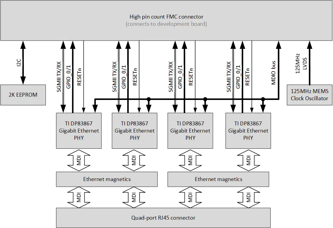
Note that the level translators are left out of the diagram for simplicity.
Level translation
To support a wide range of I/O voltages (VADJ), the Ethernet FMC Max uses level translators for the MDIO bus, the PHY reset signals and the PHY GPIO_0/1 signals. The table below lists the devices used:
| Device | Purpose |
|---|---|
| LSF0102DQER | Level translation of the shared PHY MDIO bus. |
| SN74AVC4T245RSVR | Level translation of PHY resets and GPIO_0/1. |
The other signals, such as SGMII TX/RX and the 125MHz LVDS clock, connect to gigabit transceivers that are independent of the VADJ voltage used and do not need voltage translation.
The I/O power supply of the TI DP83867 Ethernet PHYs is connected to 3.3VDC.
SGMII
The Serial GMII interfaces form the connection between the Ethernet PHYs and the MACs that are implemented in the FPGA or SoC on the development board. The SGMII interface is serial gigabit interface composed of two differential pairs, one for transmit and one for receive. The SGMII interfaces connect to the first four gigabit transceivers of the FMC connector (DP0-3).
| Port | Signal direction | FMC gigabit transceiver |
|---|---|---|
| P0 | FPGA to link partner | DP0_C2M_P/N |
| Link partner to FPGA | DP0_M2C_P/N | |
| P1 | FPGA to link partner | DP1_C2M_P/N |
| Link partner to FPGA | DP1_M2C_P/N | |
| P2 | FPGA to link partner | DP2_C2M_P/N |
| Link partner to FPGA | DP2_M2C_P/N | |
| P3 | FPGA to link partner | DP3_C2M_P/N |
| Link partner to FPGA | DP3_M2C_P/N |
As the SGMII signals connect to gigabit transceivers, they are independent of the VADJ voltage being used and do not need voltage translation.
MDIO (PHY Configuration)
The MDIO interface is used to configure the registers of the Ethernet PHYs. More information regarding the registers can be found in the DP83867 datasheet .
The mezzanine card has a single shared MDIO bus to allow configuration of the PHYs. A level translator ( LSF0102DQER ) converts the VADJ voltage levels on the side of the FPGA to the 3.3VDC voltage levels on the side of the PHYs. The MDIO bus is composed of two signals:
- MDIO Clock signal (driven by the FPGA)
- MDIO Data signal (bidirectional)
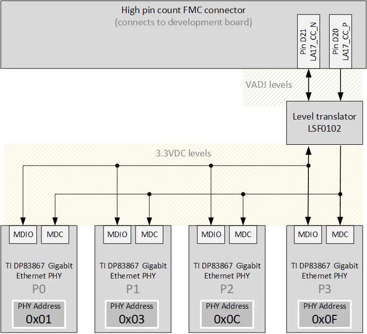
The diagram above illustrates the MDIO bus connections and the level translation. Note that the MDIO pull up resistors are left out of the diagram for simplicity.
The table below lists the MDIO bus signals and their connections to the FMC connector.
| Bus signal | Description | Direction | FMC pin |
|---|---|---|---|
| MDC | MDIO clock | FPGA to PHY | LA17_CC_P |
| MDIO | MDIO data | Bidirectional | LA17_CC_N |
Each Ethernet PHY has a fixed address that is used when targetting the PHY for MDIO transactions. The table below lists the ports and the corresponding PHY addresses:
| Port label | PHY address (binary) | PHY address (hex) |
|---|---|---|
| P0 (Port 0) | 00000001 | 0x01 |
| P1 (Port 1) | 00000011 | 0x03 |
| P2 (Port 2) | 00001100 | 0x0C |
| P3 (Port 3) | 00001111 | 0x0F |
The DP83867 datasheet specifies a maximum MDIO clock frequency of 25MHz.
PHY Resets
Each of the 4x Ethernet PHYs have an active-low reset input that can be driven (optionally) by the FPGA to hard reset the PHY. The reset signals have pull-up resistors to ensure that the PHYs are released from reset in the case that the FPGA leaves these pins floating or does not drive them. The reset signals pass through a level translator ( SN74AVC4T245RSVR ) to convert the VADJ signal levels from the FPGA to the 3.3V signal levels of the PHY.
The resets are connected to the following FMC pins:
| Port label | Reset signal name | FMC pin |
|---|---|---|
| P0 (Port 0) | E0_RESET_N_T | LA12_P |
| P1 (Port 1) | E1_RESET_N_T | LA12_N |
| P2 (Port 2) | E2_RESET_N_T | LA11_P |
| P3 (Port 3) | E3_RESET_N_T | LA11_N |
PHY GPIO Outputs
Each of the Ethernet PHYs have two multi-purpose outputs labelled GPIO_0 and GPIO_1. Despite the name “GPIO”, these pins can only be configured outputs to the PHY. Their operational mode can be configured by writing to GPIO Mux Control Register (GPIO_MUX_CTRL, address 0x0172) of the PHYs (see the DP83867 datasheet for more information). The GPIO outputs can signal such events as Wake-on-LAN, 1588 Start of Frame and receive errors. Level translators ( SN74AVC4T245RSVR ) are used to convert the 3.3V levels from the PHY to VADJ levels required by the FPGA.
By default, the GPIO outputs have the following functionality:
| GPIO | Output | Description |
|---|---|---|
| GPIO_0 | RX_ER | Receive error |
| GPIO_1 | COL | Collision detect |
The GPIO pins are connected to the following FMC pins for use by the FPGA:
| Port | Net | Description | FMC pin |
|---|---|---|---|
| P0 (Port 0) | E0_GPIO0_T | PHY GPIO0 output | LA08_P |
| P0 (Port 0) | E0_GPIO1_T | PHY GPIO1 output | LA08_N |
| P1 (Port 1) | E1_GPIO0_T | PHY GPIO0 output | LA07_P |
| P1 (Port 1) | E1_GPIO1_T | PHY GPIO1 output | LA07_N |
| P2 (Port 2) | E2_GPIO0_T | PHY GPIO0 output | LA16_P |
| P2 (Port 2) | E2_GPIO1_T | PHY GPIO1 output | LA16_N |
| P3 (Port 3) | E3_GPIO0_T | PHY GPIO0 output | LA15_P |
| P3 (Port 3) | E3_GPIO1_T | PHY GPIO1 output | LA15_N |
LVDS Clock
The Ethernet FMC Max has a 125MHz crystal oscillator ( Skyworks, Si511 ) to provide the FPGA gigabit transceivers with a reference clock that meets all stability and jitter specifications for Gigabit Ethernet. The oscillator outputs an LVDS clock and connects to the pins listed in the table below:
| Clock signal | Si511 pin | FMC pin |
|---|---|---|
| 125MHz LVDS positive | CLK_P | GBTCLK0_M2C_P |
| 125MHz LVDS negative | CLK_N | GBTCLK0_M2C_N |
Power Supplies
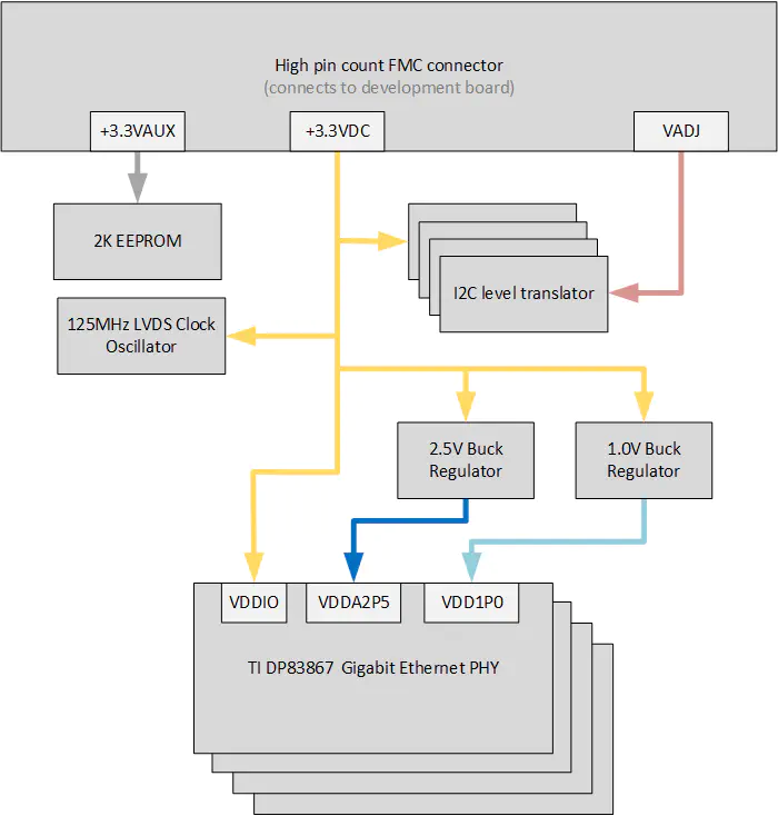
All power required by the Ethernet FMC Max is supplied by the development board through the FMC connector:
- +12VDC
- +3.3VDC
- VADJ: 1.2VDC, 1.5VDC, 1.8VDC or 2.5VDC
- +3.3VAUX
3.3VDC Supply
The 3.3VDC supply is the main power supply for the Ethernet FMC Max, it is used to power the I/O power supply (VDDIO) of the 4x TI DP83867 PHYs, as well as the 125MHz clock oscillator. The 3.3VDC supply also feeds the buck converters that generate 1.0VDC and 2.5VDC that are also required by the Ethernet PHYs.
VADJ Supply
The VADJ supply is the FPGA I/O power supply and it determines the voltage levels of the FMC I/Os. The Ethernet FMC Max uses level translators on all applicable FPGA I/Os to allow a wide range of I/O voltages to be used. The Ethernet FMC Max can support a VADJ voltage of 1.2VDC, 1.5VDC, 1.8VDC or 2.5VDC.
Power LED and testpoints
A single green LED on the Ethernet FMC Max is used to indicate when the carrier board has signaled that the FMC power supplies are active. This LED is connected through a logic buffer to the POWER GOOD signal that is driven by the carrier board and is part of the Vita 57.1 FMC standard.
To aid hardware debug, there is a test point for the 3.3VDC, 1.0VDC and 2.5VDC power supplies on the back side of the Ethernet FMC Max. The testpoint labelled GND is connected to the system ground and should be used as the reference when probing the other testpoints. Note that the RJ45 connector chassis is connected to a chassis ground that is isolated from the system ground.
3.3VAUX Supply
The 3.3VAUX supply is used to power the IPMI EEPROM and is independent of the main 3.3VDC supply so that the carrier board can read from the EEPROM without having to power up the entire board.
Clocks
The figure below illustrates the clock connections on the Ethernet FMC Max.
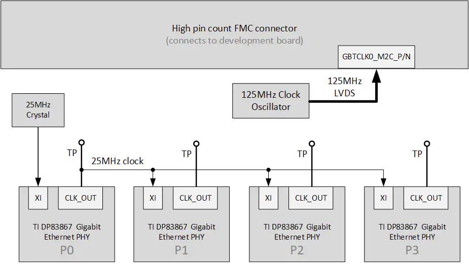
The PHY of the first port (P0) is connected to a 25MHz crystal for generation of it’s own internal clocks. By default, the CLK_OUT pin of this PHY outputs a buffered 25MHz clock that is synchronous to the crystal input. This clock output is connected to the XI (clock input) pins of the remaining 3 PHYs.
The CLK_OUT outputs are not routed to the FMC connector and are not available to the FPGA. They are however connected to test points on the back side of the mezzanine card for debugging purposes. The CLK_OUT testpoints are unlabelled and are located in the region of the decoupling capacitors.
The Ethernet FMC Max also has a 125MHz clock oscillator with LVDS output to provide the FPGA gigabit transceivers with a precision reference clock.