Detailed Description
Hardware Overview
The figure below illustrates the various hardware components that are located on the top-side (component side) of the Quad SFP28 FMC.
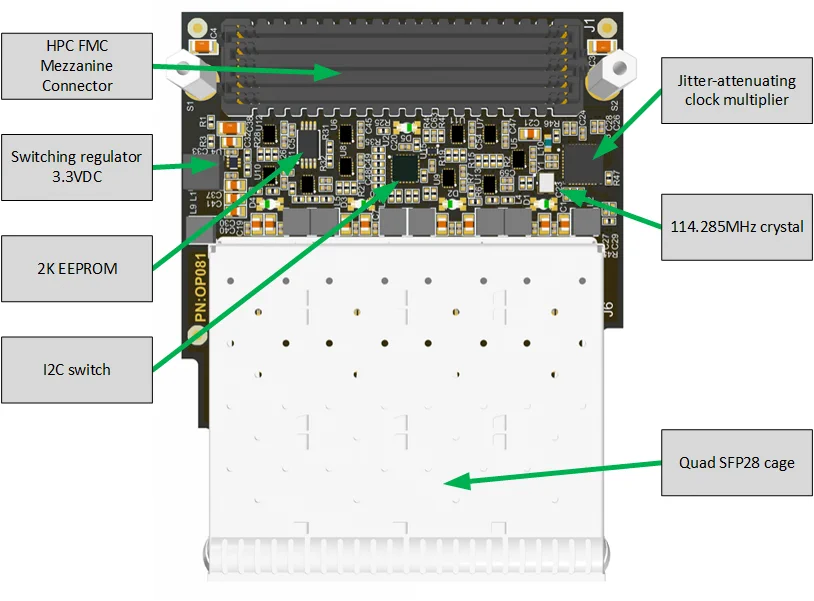
The main components on the top-side of the mezzanine card are:
- Quad SFP28 cage
- High Pin Count FMC Connector
- 2K EEPROM
- Jitter-attenuating clock multiplier ( Si5328 )
- 114.285MHz crystal
- I2C switch
- Level translators
- 3.3VDC switching buck regulator
The figure below illustrates the various hardware components that are located on the bottom-side of the mezzanine card.
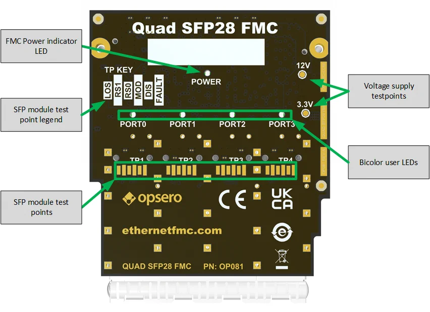
The main components on the bottom-side of the mezzanine card are:
- Bicolor user LEDs
- FMC Power indicator LED
- Test points for 12VDC and 3.3VDC power supplies
- Test points for SFP module I/Os
- Key/legend for SFP I/O test points
Quad SFP28 Cage
The SFP28 cage ( Link-PP, SFP28 Quad Cage, LP14CC01000S ) can accommodate 4x SFP, SFP+ or SFP28 modules.
Jitter-attenuating Clock Multiplier
The Quad SFP28 FMC features a jitter-attenuating clock multiplier ( Skyworks, Si5328 ), which generates two precision clocks with selectable frequencies ranging from 8kHz to 808MHz. Its wide frequency range and exceptional jitter performance support a variety of applications, including Synchronous Ethernet.
The Si5328 utilizes a 114.285MHz crystal and oscillator circuit to generate frequencies between 8kHz and 808MHz. The clock multiplication ratio can be programmed through an I2C interface. The device also has a clock input, connected to FPGA I/O pins (LA00_CC_P/N), which can receive a recovered clock from the FPGA gigabit transceivers. In Synchronous Ethernet applications, jitter attenuation can be applied to the recovered clock, which can then be directed to the clock outputs to drive the gigabit transceivers.
See the Clocks section for more information on the clock system.
EEPROM
The 2K EEPROM stores IPMI FRU data that can be read by the carrier board and contains the following information:
- Manufacturer name (Opsero Electronic Design Inc.)
- Product name
- Product part number
- Serial number
- Power supply requirements
The FRU data is read by some carrier boards to determine the correct VADJ voltage to apply to the mezzanine card. All Opsero FMC products have their EEPROMs programmed with valid FRU data to allow these carrier boards to correctly power them.
High Pin Count FMC Connector
The Quad SFP28 FMC has a low pin count FMC (FPGA Mezzanine Card) connector for interfacing with an FPGA or SoC development board. The part number of this connector is Samtec, Mezzanine-side High pin count FMC Connector, ASP-134488-01 . The pinout of this connector conforms to the VITA 57.1 FPGA Mezzanine Card Standard. For the pinout details, see the Pin configuration section. For more information on the FMC connector and the VITA 57.1 standard, see the Samtec page on VITA 57.1 .
I/O Interfaces
The FMC connector provides power to the Quad SFP28 FMC and also presents the following I/O signals to the FPGA fabric of the development board:
- Gigabit serial links for the 4x SFP28 slots
- SFP I/O signals (FAULT, TX_DISABLE, MOD, RS0/1, LOS) for the 4x SFP28 slots
- I2C for IPMI EEPROM
- I2C (PL) for SFP28 slots and clock multiplier via an I2C switch
- LVDS recovered clock from the FPGA to drive the clock multiplier
- LVDS configurable clock from the clock multiplier
- Clock loss alarm from the clock multiplier
- Drive signals for the 4x bicolor user LEDs
- Reset signal for the I2C switch
The figure below illustrates the connections to the FMC connector.
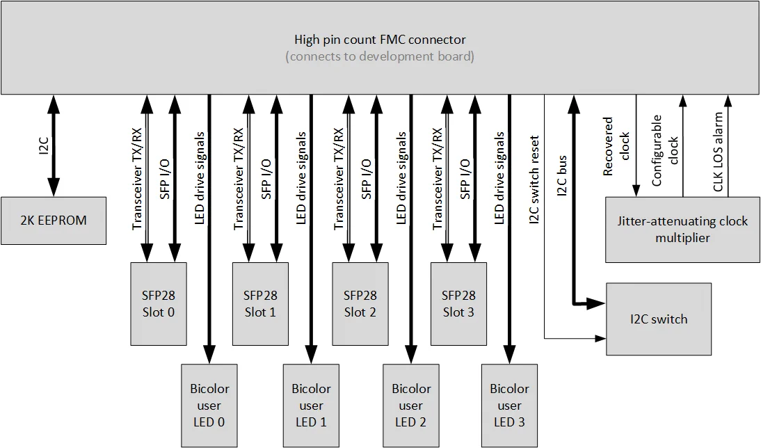
The I2C connections from the I2C switch to the slave devices has been left out of the above diagram for clarity. Details on the I2C connections can be found in the I2C Buses section.
The level translators have been left out of the above diagram for clarity. Details can be found in the Level translation section.
Level translation
To support a wide range of I/O voltages (VADJ), the Quad SFP28 FMC uses level translators for the SFP I/O signals, the PL I2C bus signals, the I2C switch reset signal, the LED drive signals and the clock loss alarm signal. The table below lists the devices used:
| Device | Purpose |
|---|---|
| TCA9416 | Level translation of the PL I2C bus. |
| SN74AVC4T245RSVR | Level translation of SFP I/Os, I2C switch reset signal, LED drive signals and clock loss alarm. |
The gigabit serial links of the SFP28 slots and the reference clocks connect to the gigabit transceivers, which are independent of the VADJ voltage and do not need voltage translation. The recovered clock signal (REC_CLK1_P/N) should be configured as an LVDS output in the FPGA and also does not require voltage translation.
Gigabit transceivers
The data channel between the SFP, SFP+, and SFP28 modules and the FPGA operates over serial gigabit links at speeds of up to 25 Gbps. The Quad SFP28 FMC connects these serial links to gigabit transceivers in the FPGA or SoC on the development board. Each serial link consists of two differential pairs: one for transmission and one for reception. These serial links connect to the first four gigabit transceivers on the FMC connector (DP0-3).
| SFP28 Slot | Signal direction | FMC gigabit transceiver |
|---|---|---|
| 0 | FPGA to link partner | DP0_C2M_P/N |
| Link partner to FPGA | DP0_M2C_P/N | |
| 1 | FPGA to link partner | DP1_C2M_P/N |
| Link partner to FPGA | DP1_M2C_P/N | |
| 2 | FPGA to link partner | DP2_C2M_P/N |
| Link partner to FPGA | DP2_M2C_P/N | |
| 3 | FPGA to link partner | DP3_C2M_P/N |
| Link partner to FPGA | DP3_M2C_P/N |
As the serial links connect to gigabit transceivers, they are independent of the VADJ voltage being used and do not need voltage translation.
SFP I/O Signals
In addition to the high-speed serial link, SFP modules have several I/O signals used for configuration and fault indication. On the Quad SFP28 FMC, these I/O signals are connected through level translators to the FPGA I/O, allowing the FPGA to control and read them. The I/O signals and their functionality are listed in the table below:
| SFP pin | Name | Direction | Function |
|---|---|---|---|
| 2 | TX_FAULT | SFP to FPGA | Indicates transmitter fault |
| 3 | TX_DISABLE | FPGA to SFP | Disables optical output |
| 6 | MOD_ABS | SFP to FPGA | Indicates module absence |
| 7 | RS0 | FPGA to SFP | Rate select 0 |
| 8 | RX_LOS | SFP to FPGA | Indicates receiver loss of signal |
| 9 | RS1 | FPGA to SFP | Rate select 1 |
The SFP I/O signals connect to the FMC pins listed in the table below:
| Slot | Net Name | FMC pin |
|---|---|---|
| 0 | SFP0_TX_DISABLE_T | LA03_P |
| SFP0_TX_FAULT_T | LA03_N | |
| SFP0_LOS_T | LA04_P | |
| SFP0_MOD_ABS_T | LA04_N | |
| SFP0_RS1_T | LA02_P | |
| SFP0_RS0_T | LA02_N | |
| 1 | SFP1_TX_DISABLE_T | LA12_P |
| SFP1_TX_FAULT_T | LA12_N | |
| SFP1_LOS_T | LA07_P | |
| SFP1_MOD_ABS_T | LA07_N | |
| SFP1_RS1_T | LA08_P | |
| SFP1_RS0_T | LA08_N | |
| 2 | SFP2_TX_FAULT_T | LA15_P |
| SFP2_TX_DISABLE_T | LA15_N | |
| SFP2_LOS_T | LA09_P | |
| SFP2_MOD_ABS_T | LA09_N | |
| SFP2_RS1_T | LA10_P | |
| SFP2_RS0_T | LA10_N | |
| 3 | SFP3_TX_FAULT_T | LA17_CC_P |
| SFP3_TX_DISABLE_T | LA17_CC_N | |
| SFP3_LOS_T | LA18_CC_P | |
| SFP3_MOD_ABS_T | LA18_CC_N | |
| SFP3_RS1_T | LA14_P | |
| SFP3_RS0_T | LA14_N |
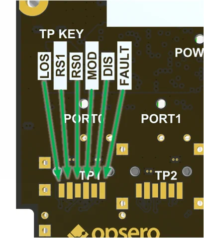
All of the SFP I/O signals are brought out to rectangular test points as a debugging aid. These test points are accessible on the bottom side of the mezzanine card and are illustrated in the bottom labelled image above. For identifying the SFP I/O signals, a key/legend is displayed on the bottom side of the mezzanine card. The signal names in the legend correspond to the test points below them, arranged in the same order and orientation as the legend. Each SFP28 slot has its own set of test points corresponding to these signals. The image below illustrates the matching between the signal names in the key and the test points for slot 0.
I2C Buses
The Quad SFP28 FMC has two independent I2C buses: the FMC’s dedicated I2C bus for the IPMI EEPROM and the PL (programmable logic) I2C bus that connects to all other I2C devices.
EEPROM I2C
A 2K EEPROM is located on the FMC card’s dedicated I2C bus. The FMC pins of the I2C bus are shown below, and it is up to the user to determine their corresponding connections to the FPGA/MPSoC on the carrier board being used.
| I2C bus signal | FMC pin name | FMC pin number |
|---|---|---|
| SCL (clock) | SCL | C30 |
| SDA (data) | SDA | C31 |
PL I2C
The main I2C bus of the Quad SFP28 FMC is implemented using two FPGA I/O pins (LA11_P/N) and enables communication between the FPGA, the four SFP28 modules, and the clock multiplier. To avoid I2C address conflicts, an I2C switch ( TI, 8-channel I2C Switch with Reset, PCA9548ARGER ) is used to connect these devices, as identical SFP28 modules may share the same address. The diagram below illustrates the I2C bus connections through the I2C switch:
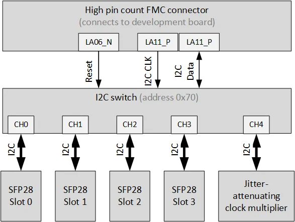
The I2C switch is wired to have I2C address 0x70, and it can be configured to target one of the lower slave devices by specifying the appropriate channel (0-4). The connected slave devices and their channels are listed in the table below:
| I2C Device | Switch channel | Device I2C address |
|---|---|---|
| SFP28 Slot 0 | 0 | Module dependent |
| SFP28 Slot 1 | 1 | Module dependent |
| SFP28 Slot 2 | 2 | Module dependent |
| SFP28 Slot 3 | 3 | Module dependent |
| Clock multiplier | 4 | 0x68 |
Note that the I2C address of the SFP28 slots will depend on the SFP/SFP+/SFP28 module that is connected to the slot. Refer to the module datasheet for the I2C address and register details.
The I2C bus signals are connected to the FMC pins listed in the table below:
| Net Name | Description | FMC pin |
|---|---|---|
| PL_I2C_SCL_T | I2C clock (SCL) | LA11_P |
| PL_I2C_SDA_T | I2C data (SDA) | LA11_N |
The PL I2C bus signals pass through a level translator to convert the FPGA I/O levels (VADJ) to 3.3VDC levels.
Clock signals
Refer to the Clocks section for more information about the clock related signals and how they connect to the jitter-attenuating clock multiplier.
Bicolor User LEDs
The Quad SFP28 FMC features four bicolor (green/red) LEDs, one for each SFP28 slot, which can be driven by the FPGA and are visible on the bottom side of the mezzanine card. These LEDs provide the user or developer with programmable visible outputs that can be linked to specific signals for monitoring. Examples of such signals for monitoring include the SFP I/Os (FAULT, TX_DISABLE, MOD, RS0/1, LOS) or other SFP module-specific indicators.
The drive pins for the user LEDs are routed through level translators to convert the FPGA I/O signal levels (VADJ) to 3.3VDC levels for driving the LEDs. The level translators have sufficient output current capacity to drive the LEDs directly.
The bicolor user LEDs connect to the FMC pins listed in the table below:
| Aligned with slot | Net Name | FMC pin |
|---|---|---|
| 0 | SFP0_GRN_LED_T | LA01_CC_P |
| SFP0_RED_LED_T | LA01_CC_N | |
| 1 | SFP1_GRN_LED_T | LA05_P |
| SFP1_RED_LED_T | LA05_N | |
| 2 | SFP2_GRN_LED_T | LA16_P |
| SFP2_RED_LED_T | LA16_N | |
| 3 | SFP3_GRN_LED_T | LA13_P |
| SFP3_RED_LED_T | LA13_N |
Power Supplies
All power required by the Quad SFP28 FMC is supplied by the development board through the FMC connector:
- +12VDC
- VADJ: +1.2VDC, +1.5VDC, +1.8VDC, +2.5VDC or +3.3VDC
- +3.3VAUX
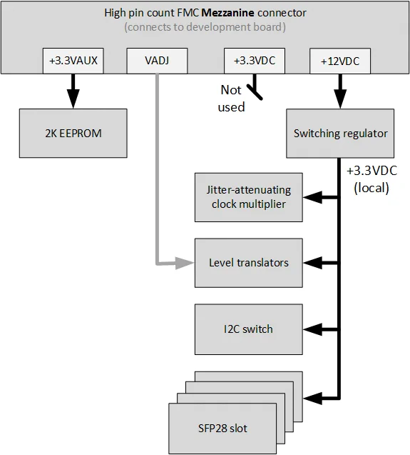
The FPGA/MPSoC carrier board also supplies a 3.3VDC power supply, however this supply is not used by the Quad SFP28 FMC.
The 12VDC Supply
The 12VDC supply is the main power source for the mezzanine card. It feeds a buck switching regulator ( TI, 5A Synchronous Buck Converter, TPS565247DRLR ) that generates 3.3VDC to power to all four SFP28 slots, the clock multiplier, the I2C switch and the level translators.
VADJ Supply
The VADJ supply is the FPGA I/O power supply and it determines the voltage levels of the FMC I/Os. On the Quad SFP28 FMC, the VADJ supply powers the level translators that allow the board to be used at any I/O voltage in the range of 1.2VDC to 3.3VDC.
The 3.3VAUX Supply
The 3.3VAUX supply is used to power the IPMI EEPROM and is independent of the main 3.3VDC supply so that the carrier board can read from the EEPROM without having to power up the entire board.
Power LED and testpoints
An LED indicates when both the power from the carrier board and the switching regulator are active, and it can be seen in the labelled bottom view of the board above. This LED is connected through a logic buffer to the POWER GOOD signal that is driven by the carrier board and is part of the Vita 57.1 FMC standard. The logic buffer is powered by the 3.3VDC that is generated by the switching regulator.
To aid hardware debug, there is a test point for the 12VDC and 3.3VDC (buck regulator) power supplies on the back side of the Quad SFP28 FMC. When probing these test points, the SFP28 cage can be used as the ground reference as it connects to the system ground.
Clocks
The clock architecture of the Quad SFP28 FMC is based on the jitter-attenuating clock multiplier ( Skyworks, Si5328 ). This clock multiplier operate in a free-running mode, generating a user-specified frequency ranging from 8kHz to 808MHz, synthesized by a crystal oscillator. In Synchronous Ethernet applications, it can also generate a jitter attenuated clock that is synchronous with link partner’s clock.
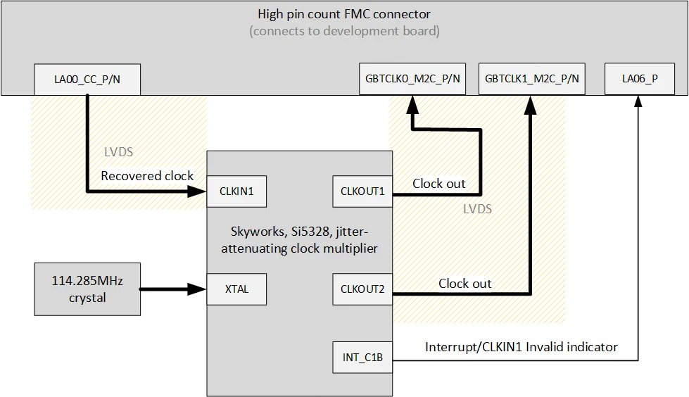
The figure below illustrates the clock connections on the Quad SFP28 FMC.
Clock outputs
The Si5328 has two output clocks, both connected to the FMC connector’s GT reference clock inputs. These clocks are divided down separately from a common source, allowing them to be programmed to different frequencies while remaining synchronous.
The clock outputs are connected to the FMC pins listed in the table below:
| Si5328 pin | I/O standard | FMC pin |
|---|---|---|
| CLKOUT1 | LVDS | GBTCLK0_M2C_P/N |
| CLKOUT2 | LVDS | GBTCLK1_M2C_P/N |
Clock input
The Si5328 has two input clocks, but only one is connected on the Quad SFP28 FMC. This clock input is connected to the FMC pins LA00_CC_P/N, enabling the FPGA to forward a recovered clock from the gigabit transceivers. The Si5328 can perform jitter attenuation on the recovered clock and forward the resulting clock to its outputs. This feature allows the Quad SFP28 FMC to be used in Synchronous Ethernet applications.
The clock inputs are connected to the FMC pins listed in the table below:
| Si5328 pin | I/O standard | FMC pin |
|---|---|---|
| CLKIN1 | LVDS | LA00_CC_P/N |
Clock loss alarm
The Si5328 has a logic output INT_C1B that indicates loss-of-signal on the input clock CLKIN1 (the recovered clock). The signal goes HIGH when the device detects missing pulses on the input clock. The clock loss alarm passes through level translation and connects to FMC pin LA06_P.

